
(updated: 06/21/2021)
LPKF provides a wide variety of through-hole plating solutions, such as mechanical through-hole plating of simple boards, semiautomatic dispensing of conductive paste for double-sided printed circuit boards, and galvanic through-hole plating of complex printed circuit boards.
- Electroplating: LPKF Contac RS and MiniContac RS electroplating system for creating multilayer printed circuit boards.
- Chemical-free: LPKF ProConduct conductivity solution without chemicals. Simple-to-use and perfect for small fabrication runs.
- Manual: LPKF EasyContac provides manual through-hole conductivity for double-sided circuit boards.
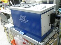
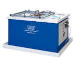
The LPKF MiniContac RS is a through-hole plating system specially developed for the professional production of prototype and small batch production printed circuit boards. The system is ideal for any rapid PCB prototyping situation, especially small runs and tight work locations. No analysis or special chemical knowledge are needed.
The system uses switchable reverse pulse plating, producing more uniform copper plating for difficult aspect ratios and smaller holes.
The LPKF MiniContac RS handles circuit boards as large as 230 x 330 mm (9.0" x 13.0"). The system is completely closed and needs no external connection.
| Device | A through-hole plating system |
| Manufacturer | LPKF Laser & Electronics |
| Model | MiniContac RS |
| Function | Electroplating machine |
| Maximum size of base material | 230 x 330 mm |
| Maximum size of circuit board | 200 x 260 mm |
| Power supply | 230 V +15/-30 % at 50-60 Hz 115 V +15/-30 % at 50-60 Hz, 400 VA |
| Dimensions (W x L x H) | 750 x 500 x 525 mm |
| Weight | 47 kg (tank empty) |
| Ambient temperature | 15 - 25 oC |
| Chemicals |  |
| ViaCleaner |  |
Interconnection of two or more layers is an indispensable part of PCB prototyping. The compact LPKF Contac S4 with six baths reliably performs this task: the board is passed through each stage of a bath cascade. This yields reliable copper layers on the surfaces of all existing vias, even in multilayer boards. The Contac S4 can process up to eight layers with a maximum aspect ratio of 1:10 (hole diameter to PCB thickness). The LPKF Contac S4 offers a subsequent tin bath step for surface protection and improved solderability.
The LPKF Contac S4 incorporates powerful techniques for improving copper layer buildup. Optimized anode plate and pulse reverse plating ensure homogeneous deposition, and carbon activation using black hole technology, integrated air blow-in, and an additional process step for via cleaning ensure reliable connections to the copper surface without the problem of layer detachment. The result is a homogeneous layer thickness in the holes and on the flat metal surface of the substrate.
The integrated touch panel with wizard and parameter administration safely guides even inexperienced users through the galvanization process. Ambitious developers can customize the settings at any time. The process requires no knowledge of chemistry and no bath analyses, as the system automatically indicates the necessary maintenance steps. Another new feature is the chemical-resistant housing with improved resistance to discoloration – the Contac S4 combines functionality, good looks, and practicality.
| Device | A through-hole plating system |
| Manufacturer | LPKF Laser & Electronics |
| Model | Contact S4 |
| Function | Electroplating machine |
| Maximum size of base material | 230 x 330 mm |
| Maximum size of circuit board | 200 x 260 mm |
| Reverse pulse plating | Adjustable |
| Tolerance | ± 2 μm (plated copper) |
| Minimum hole diameter | ≥0.2 mm (≥7.8 mil) |
| ViaCleaner | Included |
| Chemical tinning | Included |
| Process time | Approx. 90 – 120 min |
| Electrical consumption | 110/230 V, 50 – 60 Hz, single phase, 0.75 kVA |
| Dimensions (W x L x H) | 856 x 446 x 542 mm |
| Weight | 80 kg unfilled, ~115 kg filled |
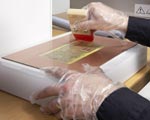
The LPKF ProConduct® introduces revolutionary technology to produce plated through-holes, which does not require a plating tank or potentially hazardous processing chemicals. This compact system is extremely fast and easy to use. Its rapid parallel processing method delivers completely safe, reliable and thermally stable via plating results for double-sided or multilayer boards.
Circuit board prototypes can be easily fabricated in-house in a single day when the LPKF ProConduct® system is combined with an LPKF ProtoMat circuit board plotter.
In-house PCB prototyping gets your designs to market faster by eliminating production delays and high costs that can occur with outside vendors. It also makes your precious design data secure by keeping it under your control.
LPKF ProConduct® uses specially-developed plating technology to rapidly plate vias as small as 0.4 mm (15 mil) up to aspect ratio of 1:4. Even smaller holes are possible under special conditions. The entire process can be completed in just a few minutes for double-sided and even multilayer boards. The electrical resistance of LPKF ProConduct® plating is extremely low with 19.2 mOhm depending on the material thickness.
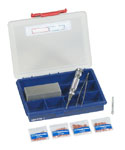
LPKF EasyContac is a simple and easy to operate system for circuit board through-hole plating. Minor production effort and low costs are the major benefits of this manual solution.
LPKF EasyContac is particularly suitable where two-sided soldering is not possible, such as beneath components. The EasyContac set contains all of the necessary tools and materials, with the exception of a soldering iron.